How to tap the sun’s energy through heat as well as light
New approach developed at MIT could generate power from sunlight efficiently and on demand.
A new approach to harvesting solar energy, developed by MIT
researchers, could improve efficiency by using sunlight to heat a
high-temperature material whose infrared radiation would then be
collected by a conventional photovoltaic cell. This technique could also
make it easier to store the energy for later use, the researchers say.
In this case, adding the extra step improves performance, because it
makes it possible to take advantage of wavelengths of light that
ordinarily go to waste. The process is described in a paper published
this week in the journal Nature Nanotechnology, written by
graduate student Andrej Lenert, associate professor of mechanical
engineering Evelyn Wang, physics professor Marin Soljačić, principal
research scientist Ivan Celanović, and three others.
A conventional silicon-based solar cell “doesn’t take advantage of all
the photons,” Wang explains. That’s because converting the energy of a
photon into electricity requires that the photon’s energy level match
that of a characteristic of the photovoltaic (PV) material called a
bandgap. Silicon’s bandgap responds to many wavelengths of light, but
misses many others.
To address that limitation, the team inserted a two-layer
absorber-emitter device — made of novel materials including carbon
nanotubes and photonic crystals — between the sunlight and the PV cell.
This intermediate material collects energy from a broad spectrum of
sunlight, heating up in the process. When it heats up, as with a piece
of iron that glows red hot, it emits light of a particular wavelength,
which in this case is tuned to match the bandgap of the PV cell mounted
nearby.
This basic concept has been explored for several years, since in
theory such solar thermophotovoltaic (STPV) systems could provide a way
to circumvent a theoretical limit on the energy-conversion efficiency of
semiconductor-based photovoltaic devices. That limit, called the
Shockley-Queisser limit, imposes a cap of 33.7 percent on such
efficiency, but Wang says that with TPV systems, “the efficiency would
be significantly higher — it could ideally be over 80 percent.”
There have been many practical obstacles to realizing that potential;
previous experiments have been unable to produce a STPV device with
efficiency of greater than 1 percent. But Lenert, Wang, and their team
have already produced an initial test device with a measured efficiency
of 3.2 percent, and they say with further work they expect to be able to
reach 20 percent efficiency — enough, they say, for a commercially
viable product.
The design of the two-layer absorber-emitter material is key to this
improvement. Its outer layer, facing the sunlight, is an array of
multiwalled carbon nanotubes, which very efficiently absorbs the light’s
energy and turns it to heat. This layer is bonded tightly to a layer of
a photonic crystal, which is precisely engineered so that when it is
heated by the attached layer of nanotubes, it “glows” with light whose
peak intensity is mostly above the bandgap of the adjacent PV, ensuring
that most of the energy collected by the absorber is then turned into
electricity.
In their experiments, the researchers used simulated sunlight, and found
that its peak efficiency came when its intensity was equivalent to a
focusing system that concentrates sunlight by a factor of 750. This
light heated the absorber-emitter to a temperature of 962 degrees
Celsius.
This level of concentration is already much lower than in previous
attempts at STPV systems, which concentrated sunlight by a factor of
several thousand. But the MIT researchers say that after further
optimization, it should be possible to get the same kind of enhancement
at even lower sunlight concentrations, making the systems easier to
operate.
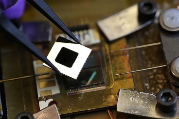
 A nanophotonic solar thermophotovoltaic device composed of an array of multi‑walled carbon nanotubes as the absorber, a one‑dimensional silicon/silicon dioxide photonic crystal as the emitter, and a 0.55 eV photovoltaic cell.
Photo: John Freidah
Some of the ways to further improve the system are quite straightforward. Since the intermediate stage of the system, the absorber-emitter, relies on high temperatures, its size is crucial: The larger an object, the less surface area it has in relation to its volume, so heat losses decline rapidly with increasing size. The initial tests were done on a 1-centimeter chip, but follow-up tests will be done with a 10-centimeter chip, they say.
Zhuomin Zhang, a professor of mechanical engineering at the Georgia Institute of Technology who was not involved in this research, says, “This work is a breakthrough in solar thermophotovoltaics, which in principle may achieve higher efficiency than conventional solar cells because STPV can take advantage of the whole solar spectrum. … This achievement paves the way for rapidly boosting the STPV efficiency.”
The research team also included MIT graduate students David Bierman and Walker Chan, former postdoc Youngsuk Nam, and research scientist Ivan Celanović. The work was funded by the U.S. Department of Energy through MIT’s Solid-State Solar Thermal Energy Conversion (S3TEC) Center, as well as the Martin Family Society, the MIT Energy Initiative, and the National Science Foundation.
MIT; January 19, 2014
--------------------------
---------------------------
